


Scan the code and contact me


The so-called RC circuit is a voltage dividing circuit composed of resistance R and capacitance C. As shown in Figure 1 below, the input voltage is applied to both ends of RC series circuit, and the output voltage is taken from resistance R or capacitance C. Due to the special nature of capacitance, different output voltages in (a) and (b) below show different frequency characteristics.
Speaking of the difficulties of switching power supply, PCB layout is not a great difficulty, but if you want to layout a good PCB, it must be one of the difficulties of switching power supply (PCB design is not good, which may lead to debugging the layout no matter how the debugging parameters are, so it is not alarmist). The reason is that there are still many factors to be considered in PCB layout, such as electrical performance, process route, safety requirements, EMC impact, etc; Among the factors considered, electrical is the most basic, but EMC is the most difficult to understand. The bottleneck of many projects lies in EMC; Now let's share PCB layout and EMC from nine directions.
01 familiar with the circuit before you can calmly carry out EMI circuit of PCB design
Some products EMC is difficult to deal with at the source, and magnetic ring filtering can be used. Of course, the magnetic ring I mentioned here has two levels of meaning. On the one hand, it is the filter inductance at the input and output ends. Using magnetic rings of different materials and different turns will have corresponding effects. On the other hand, it is intended to directly sleeve magnetic rings on the input and output lines, which can sometimes play a wonderful role, but it can not be used in all occasions, at least it can be used as a basis for judgment;
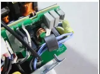
The blue and black lines in the figure above are the positive and negative ends of the output, which are covered with a magnetic ring to solve the high-frequency end excess caused by the output rectifier tube; Sometimes it may not be effective to add a filter to the PCB for port interference. Placing a magnetic ring on the output line will have an unexpected effect.
02Key signals of pcb wiring
be careful:
1.CS signal (sampling signal): pull out from the sampling resistors R25 and R26. Note that the IC ground wire is based on the sampling resistance, and the positive and negative differential wiring of the sampling resistance pulls down the IC CS pin and the IC GND pin.
2.The drive signal pulls down the IC drive pin from the drive circuit, and be careful not to interfere with the CS pin; As shown in the figure, route the three wires side by side, and route the ground wire between the drive line and the CS line to play a certain shielding role;
3.It is best to lay a layer of IC on the ground and shield the double panel. The paved network must be led out from IC GND. Non critical signal GND can be directly punched through holes. Critical signal grounding requires a single point grounding, which is directly connected to IC;
4.FB feedback network signal, pay attention to check the wiring and connect IC at a single point;
5.RCD absorption network should not be placed in the main circuit;
6.The rectifier filter ground of VCC needs to be connected to the main power ground, and the secondary filter can be connected to IC ground;
7.Y capacitor wiring shall be connected separately, which shall not be confused with the main power to avoid interference.
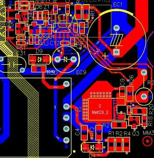
03 main power and control part grounding wiring diagram

Many people may see this picture in a fog. Let's give a general introduction:
1. PFC drive and IC are grounded together with PFC tube, and more specifically, the ground of sampling resistance;
2. The driving ground and control ground of DC-DC part are connected to the sampling ground of DC switch tube part;
3. The control ground of the auxiliary source part is connected to the auxiliary source MOS tube sampling section, and the MOS tube ground is then connected to the main power ground;
4. The power supply ground of each IC is connected to the IC through the auxiliary source EC filter. Note that the RC filter is close to the IC.
Summary: pay attention to their single point grounding, and the ground wire is not disordered, which is one of the most important places for wiring!!!
04 analysis of electromagnetic field shielding mechanism

As shown in the figure, the input and output electric field interference can be coupled through capacitance transmission. If the shielding plate is added, the size of C4 will be increased, and C1 will also be reduced, which plays the purpose of attenuation of electric field interference.

As shown in the figure: the characteristics of magnetic field shielding are different from that of magnetic field, which requires shell shielding, and the electric field only requires plane shielding plate, so the radiator shielding brings electric field shielding, and some use shell enclosed power supply to play a certain magnetic field shielding;
According to the principle of magnetic field shielding, the magnetic field will change the magnetic circuit through the shielding cover, resulting in the diffusion of the magnetic line of force around, and the interference of the intermediate magnetic field to achieve the purpose of shielding.
05 switching devices and EMC
What parameters of switching devices have an important impact on EMC? We often say fast transistors and slow transistors. What is the reference? We all know that the opening loss of fast tube is small, and we all like to use it for high efficiency, but in order to pass EMC smoothly, we have to abandon efficiency and reduce the switching speed to weaken the switching radiation;
For MOS transistors, the turn-on speed is determined by the driving resistance and the input junction capacitance; The turning off speed is determined by the output junction capacitance and the internal resistance of the tube;


Referring to the above two figures, there are different types of MOS tubes. Compare the input junction capacitance and output junction capacitance, 2400pf and 6800pf; 780pf and 2200pf; At first glance, we can see that the first specification is fast tube and the second is slow tube. At this time, the switching speed should match the driving resistance; In general, the driving resistance is more in 10r-150r, and the selection of driving resistance is related to the junction capacitance. For Allegro, the driving resistance can be appropriately increased, and the slow tube driving resistance can be appropriately reduced;
For diodes, there are Schottky diodes, fast recovery diodes, ordinary diodes, and a less used SiC diode. The switching speed SiC diode is almost zero, which means that there is no reverse recovery, the switching radiation is minimal, and the loss is also minimal. The only disadvantage is that it is expensive, so it is rarely used; The second is Schottky diode. The forward voltage decreases and the reverse recovery time is short, followed by fast recovery and ordinary diode; Compromise between loss and EMC; Generally, measures such as changing absorption and installing magnetic beads can be taken to rectify EMC.
06emc filter
The selection of filter architecture is very important to the filter. In different occasions, the filter achieves the filtering effect according to impedance matching. You can refer to and select how to filter according to the principles of this figure; For example, π filter is used behind the most commonly used output rectifier bridge and LC filter is used at the output end;

The material of filter is also very important to the design of filter inductance. The material with different initial permeability will work in different frequency bands, and the wrong material will completely lose its due effect.
07Analysis of flyback high frequency equivalent model of emc

First understand EMC from the simplest model:
The path of EMC, of course, space radiation is related to the loop, which is also constructed by the path; Analyze the flyback high frequency equivalent model to help understand the mechanism of EMC formation; Our test receiving equipment will receive conduction from the L and N ports. In order to reduce the received interference, it is necessary to let the interference flow through the ground circuit rather than from the L and N ports to the receiving equipment; At this time, our EMI inductance and Y capacitance can be achieved through impedance matching; In addition, the interference of the primary side can be coupled to the secondary side through the Y capacitance of the primary side and the secondary side, the stray capacitance of the transformer and the earth, forming more loops; Of course, some junction capacitance parameters, such as MOS junction capacitance and radiator junction capacitance, can also form a flow path.
08 form and frequency distribution of radiation

This figure may be a little abstract, but it happens that EMC is difficult to be specific. We need to give us some enlightenment. It can be seen that differential mode radiation exists in the form of a loop, while common mode radiation is emitted in the form of an antenna; Therefore, it just confirms that when we lay boards, we should not take sharp angles when switching the layout of the loop and routing. Generally, we should take 45 degrees, preferably circular arc routing. Of course, the routing efficiency will be relatively low.
The basic knowledge of these principles is well understood, which is very useful for the actual handling of EMC work and layout. If there is no such awareness, it may be useless, because it cannot provide a direct method, and it needs to be combined with other knowledge.
Moreover, many of the principles mentioned here are not visible in many EMC materials, and they are not so centralized, which requires repeated experience!

As shown in the figure: the relationship between some frequency terminals and the generating part of switching power supply is only a general rule, so don't completely believe it; Why is it that you can't believe all the rules? The law does not hold true in all cases, and there are great differences between different power sources, so the principle is to help you analyze, rather than hard cover according to the method.
09emc instance


According to the conduction example, the key to the distribution point of frequency is the relationship between the specific data and the fundamental frequency. After this test, it is necessary to guess the law of these values and what clues may be found; Of course, the means of how to solve these frequencies through filters has also been mentioned above.
Here is to add some mysterious EMC. How did it come from? I don't feel mysterious anymore. I don't just use filters to solve the problem!
END
Source: the copyright of power R & D elite circle belongs to the original author. If there is any infringement, please contact to delete it.
